The precise control of domain wall (DW) pinning and depinning in nanowires is crucial for the operation of new spintronics devices based on DW motion. However, the engineering of appropriate pinning sites is difficult to achieve: depinning mechanisms are not clearly understood yet, especially since the pinning potential seen by the DW can be very complex. This complexity appears in particular through the stochastic behaviour of DW depinning, which has been experimentally observed in systems with perpendicular1,2,3,4,5,6 and planar magnetization7,8,9,10,11,12,13,14. This stochasticity has been also investigated using simulations or analytical models. If it could become a major challenge for practical applications, even in the nanosecond range6, it is also very sensitive to the application of currents and thus provides a way to probe spin transfer effects at low current densities2,18.
Two sources of randomness have been identified: the first one is the thermal activation1 and the second one the ability for the DW to be randomly pinned on a given defect along different micromagnetic configurations. These sources are known to affect the statistical distribution of pinning times when constant fields or currents are applied15, or the distribution of pinning fields in field sweeping experiments14.
In the following, we study DW depinning under field and/or current, in nanowires with both perpendicular (FePt) and planar (NiFe) magnetization. Using different kind of constriction to pin the DW, we show that although the observed behaviour is often complex, we can provide a unified picture of stochastic depinning by identifying three elementary behaviours as the building blocks of any depinning mechanism.
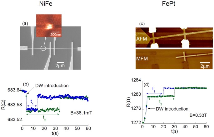
FePt-based spin-valves [FePt(5 nm)/Pd(2 nm)/FePt(5 nm)//MgO] with high perpendicular anisotropy have been grown by molecular beam epitaxy16. 30 nm thick NiFe samples were deposited by e-beam evaporation. Nanowires have then been processed in both kinds of layers using e-beam lithography techniques (see Fig. 1a). The FePt and NiFe nanowires are respectively 200 nm and 100 nm wide and constrictions are patterned in order to pin the DW.
(a) SEM image of a 100 nm wide NiFe nanowire with Au pads for electrical contacts and MFM image (inset) showing a DW pinned on the 50 nm wide constriction. (b) The DW motion is detected using a resistance measurement, probing both the AMR and the MMR and a constant field is applied to the sample. A DW is introduced in the constriction, where it gets pinned for a while. The pinning time is stochastic, varying from experiment to experiment. Here are shown two examples of measurements realized using the same experimental conditions, but leading to different pinning times t1 and t2. (c) AFM and MFM images of a 200 nm wide FePt/Pd/FePt nanowire. The MFM image shows a single DW pinned on a 80 nm wide constriction. (d) Variation of the GMR as a function of time, associated to the motion of the DW between the two contacts. Here again, the two different pinning times obtained by repeating the measurement illustrate the stochastic behaviour of DW depinning.
The position of the DW along the wire is detected using transport techniques: a small AC current (J = 2.109 A/m2, f = 1023 Hz for FePt and J = 3.1010 A/m2, f = 6700 Hz for NiFe) is injected in the main wire, while a lock-in registers the voltage between two transverse contacts. A field close to the depinning field of the DW is applied, either perpendicularly to the layer (FePt) or along the main wire direction (NiFe). For NiFe devices, the DW position is then detected using a combination of Anisotropic Magneto-Resistance (AMR) and Magnon Magneto-Resistance (MMR)17 (cf. fig. 1b). For FePt devices, the spin-valve structure allows using the Giant Magneto-Resistance (GMR) effect (cf. fig. 1d). The observed signals indicate that a DW is injected from the nucleation pad, gets quickly pinned on the constriction where it stays for a while. Then a depinning event occurs, followed by DW propagation.
As the pinning time is found to be stochastic, the measurement has to be repeated several times (usually 400) in order to determine its associated probability law. Such probability laws can be represented using the cumulative distribution functions of the pinning time P