Fermi level depinning by Au1-xSex alloy
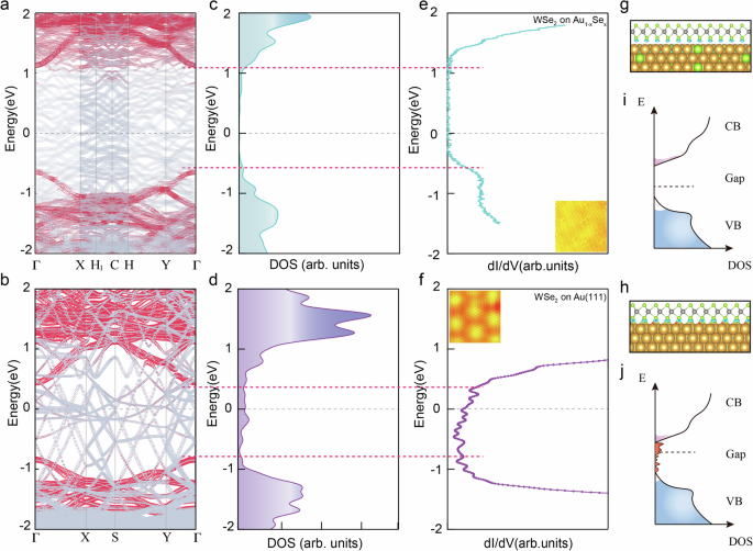
Before presenting the experimental results, we first show DFT calculations of the electronic structure of the proposed approach (see Methods for calculation details). Figure 1a displays the atomically projected band structure of 3-layer Au1-xSex in contact with a monolayer WSe2, where x = 0.10 for the specific model presented. Compared to the case of a pure Au contacted with WSe2 (Fig. 1b), the WSe2 exhibits a notable hole doping effect after made contact with Au1-xSex alloy. Specifically, as seen from Fig. 1a, the Au0.90Se0.10–WSe2 contact gives rise to a notable downward shift of the Fermi level (EF) towards the valence bands upon orbital hybridization, along with a diminishing DOS in the monolayer WSe2 energy gap. Band structures of models with different alloy compositions (x = 0.06, 0.10, 0.11, 0.25 and 0.33 in the contact layers) are presented in Supplementary Fig. 1. DFT calculations of changing alloy composition or changing the alloy layer thickness (Supplementary Fig. 2) do not reveal qualitive changes about the diminished metal-induced gap states and the hole doping effect. To elucidate the nature of band hybridization, we analyzed the projected density of states (PDOS) as shown in Supplementary Fig. 3 as well as the total DOS of the monolayer WSe2 near EF when it is in contact with Au0.90Se0.10 and Au (111), respectively (Fig. 1c, d). The calculations reveal pronounced MIGS within the bandgap and thus the propensity of FLP for the Au-WSe2 contact, whereas the alloy-WSe2 contact substantially suppresses interface states and leads to a FLP-free system. Besides, it promotes a p-type doping effect in the WSe2 monolayer. These findings show good agreement with our scanning tunneling microscopy/spectroscopy (STM/S) measurements shown in Fig. 1e and obtained from a monolayer WSe2/Au1-xSex sample flip transferred on Au using wafer bonder (see Methods and Supplementary Fig. 4 for more details). As seen from Fig. 1e, when the monolayer WSe2 is in contact with the Au1-xSex alloy, STS shows no obvious in-gap states, and the semiconductor shows a clear p-type behavior. Such a gap-state-free characteristic is similar to WSe2 on typical vdW substrates such as graphene31,32, indicating a very weak interaction at the interface. On the other hand, when the monolayer WSe2 is in contact with pure Au (111) (Fig. 1f), STS detects obvious gap-states originated from the relatively strong coupling between WSe2 and Au (111)33, and the semiconductor shows an unfavorable n-type behavior. To elucidate further the charge transfer characteristics, charge density difference calculations were carried out for both systems (Fig. 1g, h). Figure 1g clearly presents the interface charge depinning effect for the Au0.90Se0.10-WSe2 heterointerface, consistent with the above experiments and calculations. For such a model system, both the hybridization degree and charge transfer magnitude are significantly suppressed, suggesting improved vdW contact property. Bader charge analysis indicates a small electron transfer of ~2.98 × 10⁻⁵ e/Å2 from WSe2 to 3-layer Au0.90Se0.10, so p-type doping of the semiconductor is promoted in the system. This is consistent with our STS results that the Fermi level shifts towards the valence bands by ~0.5 eV when WSe2 is in contact with Au1-xSex alloy, compared to WSe2/Au, indicating a hole doping effect to monolayer WSe2. We also note, in passing, that according to our DFT calculations, a surface alloy layer is sufficient to cause MIGS-suppression and induce hole doping at the metal-semiconductor interface as presented in Supplementary Fig. 1. After all, the coupling and hybridization are dominated at the interface layers. Figure 1i, j schematically show the band alignment of WSe2 in Au1-xSex-WSe2 and Au-WSe2 configurations, illustrating effective mitigation of the FLP and induction of hole doping in WSe2 monolayer by contact with an Au1-xSex alloy.
Density-functional theory (DFT) calculated energy bands of a, Au1-xSex –WSe2 contact (x = 0.10) and b, Au-WSe2 contact, where the bands from WSe2 monolayers and metals are highlighted in red and gray respectively (Fermi level set to 0). The size of the symbols represents the relative contribution. c, d DFT calculated density of states (DOS) of WSe2 monolayers in contact with c, Au1-xSex (x = 0.10) and d, Au, respectively. e, f Scanning tunneling spectroscopy (STS) spectra (mains) and atomic resolution scanning tunneling microscopy (STM) images (insets, sizes and sample biases: e 10 nm × 10 nm, −0.50 V and f 5 nm × 5 nm, 0.03 V) measured on WSe2 monolayers in contact with e, Au1-xSex and f, Au, respectively. The baselines of differential conductance were set to 0. g, h Stick-and-ball models with charge density difference of g, WSe2 monolayers on 3-layers Au1-xSex (x = 0.10) and h, on Au, where the W atoms, Se atoms and Au atoms are colored in gray, green and yellow respectively. The isosurface was set to 0.002 e/bohr3. i, j Schematic diagrams of the DOS as extracted from c and d on i, Au1-xSex and j, Au, where the metal induced gap states (MIGS) are illustrated in red color. CB and VB represent conduction bands and valence bands respectively. To guide the eye and facilitate comparison between the calculation and experimental results, red dashed lines are drawn across Fig. 1a–f to indicate the calculated conduction band minimum (CBM) and valence band maximum (VBM), while the gray dashed lines mark the Fermi levels.
MBE growth of Au1-xSex alloy and Characterization
For device purposes, we fabricate the Au1-xSex-WSe2 contact using MBE according to the following procedure: the MOCVD-grown WSe2 films were transferred on a dielectric (HfO2) and loaded into MBE. Se films of ~3 nm thick were then deposited at a low-temperature (~−140 °C). The low substrate temperature ensured more uniform Se films covering fully the WSe2 monolayer. Deposition at room or higher temperatures resulted in severe clustering of Se, prohibiting the full coverage of WSe2 by Se (refer to Supplementary Fig. 5). In addition, low-temperature would alleviate lattice damage of WSe2 by the deposit16,34. Upon the completion of Se-film deposition, Au film was deposited at temperatures below −120 °C for a thickness of about 30 nm, after which the sample was warmed up slowly to room temperature over a period of around 2 h. Such a deposition procedure is found to produce the desired Au1-xSex contact film on WSe2 according to an array of experimental characterizations and theoretical investigation. Indeed, the propensity of Se to alloy with Au can be inferred by our ab initio molecular dynamics (AIMD) simulation results (refer to Supplementary Fig. 6), which shows that even for a stable Se (0001)-2×1 structure35, the deposited Au atoms readily displace Se atoms and dive in crystal, forming an alloy with Se. Experimentally, formation of an Au1-xSex alloy are evidenced by X-ray photoelectron spectroscopy (XPS), energy dispersive X-ray spectroscopy (EDS), three-dimensional atom probe tomography (3D-APT), electron energy loss spectroscopy (EELS), X-ray diffraction (XRD) and scanning transmission electron microscopy (STEM) measurements. The comparison of concentration estimates by 3D-APT, XPS and EDS, along with their respective characterization advantages, are summarized in Supplementary Fig. 7.
Cross-sectional annular dark-field STEM (ADF-STEM) experiments were carried out on such samples. Figure 2a, b present typical results, which reveal the atomic structure of an Au1-xSex alloy interfaced with WSe2. Since Se and Au show minimal contrast difference in cross-sectional STEM (refer to Supplementary Fig. 8 for abTEM simulated images), these micrographs unfortunately do not provide direct evidences about the atomic configuration in the alloy. However, by the homogeneity and regularity of the lattice, we suggest Se incorporation is predominantly substitutional rather than interstitials. In fact, according to our abTEM simulations, if Se occupies interstitial sites, pronounced lattice distortion and intensity variation would be shown in STEM, which we have so far failed to detect. Besides, our DFT calculations also suggest that the substitutional configuration is more energetically favorable than interstitials (Supplementary Fig. 8). In any case, the alloy film exhibited an expanded lattice according to STEM measurements. By averaging over 500 atoms in the STEM micrographs (Supplementary Fig. 9), we estimate a lattice constant of about 4.3 Å of the alloy film, which is markedly larger than that of a pure gold film deposited directly on WSe2 without the Se buffer (~4.1 Å). An expanded lattice was also verified by XRD measurements (Supplementary Fig. 10). The EELS characterizations of the contact film in the electron microscope (Supplementary Fig. 11) reveal the characteristic Se L-edge together with the Au M-edge, affirming the co-existence of Au and Se, indicating an Au1-xSex alloy. From STEM micrographs, one further notes that the alloy and WSe2 monolayer forms a sharp interface without Se residual (see, e.g., Fig. 2b), and a weakened coupling between WSe2 and Au1-xSex than that with Au may be inferred by an enlarged vdW gap that is measured to be about 2.5 Å for the case of Au1-xSex-WSe2 but 2.2 Å for the Au-WSe2 contact (see Supplementary Fig. 12). The STEM allowed us to cross check the chemical distribution profile in the sample by an elemental energy-dispersive X-ray spectroscopy (EDS) mapping and spectrum analysis as shown in Supplementary Figs. 13 and 14, again revealing a dispersed Se distribution profile throughout the Au contact layer. Separately, an independent 3D-APT measurement of a similar sample as shown in Fig. 2c provides additional direct and unambiguous evidence for the presence of Se dispersed over the film, suggesting it is an alloy of Au and Se rather than a pure Au film, and the estimated average Se content is at ~6%.
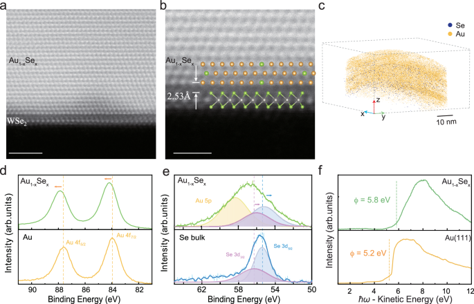
a Annular dark-field scanning transmission electron microscopy (ADF-STEM) image of the cross-section of WSe2 in contact with Au1-xSex. Scale bar, 2 nm. b Zoom-in atomic-resolution STEM image with schematic model, where W (gray), Se (green) and Au (orange) atoms are overlayed on the image. The vdW heterointerface gap is 2.5 Å wide as marked. Scale bar, 1 nm. c 2D slice view of three-dimensional atom probe tomography (3D-APT) analysis of the alloy film, showing Se and Au (colored in blue and yellow, respectively) distribution over the analyzed region. d, e X-ray photoelectron spectroscopy (XPS) characterizations of Au1-xSex, Au, and Se films, and in e, peak fitting results are also shown. f Ultraviolet photoelectron spectroscopy (UPS) spectra of Au1-xSex and Au(111).
Figure 2d, e shows typical XPS spectra of Au1-xSex alloy, which reveal a binding energy shift of the Au 4f peaks to a higher value by ~ 0.2 eV when compared with that of the bulk Au (Fig. 2d). For the Se 3d orbitals (Fig. 2e), fittings of the broader and shouldered peak resolve the Se 3d3/2 and Se 3d5/2 peaks that are red-shifted by ~ 0.2 eV in the Au1-xSex alloy than that of a MBE-grown Se film of ~20 nm thick, conforming to the bonding characteristics between Au and Se36,37. We remark that the Se peak in Fig. 2e is unlikely from WSe2 embedded in the sample, since the top Au1-xSex layer is ~30 nm thick and the measured spectrum contains no signal of W (Supplementary Fig. 15). These results suggest that Se are incorporated in Au with chemical bonding, i.e., in the form of an alloy, rather than physical mixtures or surface adsorbates. Presented in Supplementary Fig. 16 are a series of XPS results obtained at varying depths of the film by argon sputtering. It consists of 24 sputtering/probing cycles of a grown Au1-xSex/WSe2 sample (see Method). The existence of Se in the metal film can be clearly noted, where the composition estimated through peaks fitting varies between 8% to 11% across the entire thickness. To further attest the alloy, ultraviolet (UV) visible spectrum of the Au1-xSex alloy film is acquired and shown in Supplementary Fig. 17 and compared with that from pure Au and Se films. It reveals differences as well as shift of the absorption peaks, inferring certain interaction between the Se atoms with the surrounding Au atoms to lower the band energy, suggesting an alloy than mixtures of Au and Se.
Finally, ultraviolet photoelectron spectroscopy (UPS) experiments were also carried out in situ, i.e., in a chamber vacuum interlocked with the MBE reactor immediately after the sample was grown and transferred without exposing to air. The UPS spectra shown in Fig. 2f for the Au1-xSex-WSe2 and Au-WSe2 samples reveal a work function difference, ~5.8 eV for the alloy and ~5.2 eV for pure Au. The spectrum and consequently the work function of Au1-xSex alloy exhibit no change after in situ annealing at 300 °C for 2 h (Supplementary Fig. 18), suggesting firstly good thermal stability of the alloy film and secondly the spectrum is characteristic to the alloy rather than from possible surface Se contaminates, as annealing would have effectively desorbed the adsorbates, if present at all. Notably, the work function of the alloy is significantly larger than pure Au, suggesting an appealing candidate for making p-type contact with monolayer WSe238.
At this juncture, we wish to make a comment on the possible pathway under which the alloy is formed upon Au deposition on a thin pre-deposited Se film at low-temperature. Firstly, we remark that possible background Se or those evaporated from the walls of the MBE reactor acted as the source of alloy growth is ruled out, since depositing Au under the same condition but directly on WSe2 without the Se buffer layer has been found to lead to a pure Au film (Supplementary Figs. 9 and 10). In other words, the alloy must have formed by consuming the pre-deposit Se layer, which is consistent with the STEM observation that the Se layer has vanished after the Au deposition (see, e.g., Fig. 2a and b). To evaluate possible processes, we performed AIMD simulations (Supplementary Fig. 6), which showed that for the (2 × 1) surface reconstructed crystalline Se (0001)35, it remained stable at both room-temperature (300 K) and 150 K after 650 ps. When adsorbed with Au, the Se film became decomposed, and Se atoms were desorbed after 650 ps at 300 K. At the low-temperature (150 K), however, although Se atoms were also displaced, they remained in film, leading to a net effect of Au incorporation in Se. Therefore, low-temperature appears critical in order to maintain the needed Se for alloy formation, consistent with the experiments. Low-temperature also ensures Au and Se are locally trapped, prohibiting bulk diffusion or migration of atoms into pure Se and Au phases, which would otherwise be favorable due to low solubility. Based on the above, we may postulate a process as follows (Supplementary Fig. 19), but also note that it remains speculative and more systematic studies are needed to establish firmly the underlying mechanism of Au1-xSex alloy formation: after a uniform ~3 nm thick Se film is deposited on the monolayer WSe2 at low-temperature, Au is deposited from high-temperature cells, which possesses high kinetic energies capable of displacing Se and dives deeper into the Se film before becoming equilibrated with the sample temperature (150 K) and trapped inside, forming the alloy with Se. Expectedly, an optimal Se film thickness exists: too thick a film will make the Au atoms unable to reach to the very bottom of the Se layer, so besides an alloy, a residual of pure Se would remain at the interface, which is evidenced experimentally (Supplementary Fig. 20). If the Se film was too thin, the Au atoms would retain the high kinetic energy even after reaching the Se-WSe2 interface, causing damages to WSe2. Experimentally, an optimal Se film thickness about 3 nm has been identified. The Se pre-deposit layer thus not only serves as the source needed for growing the Au1-xSex alloy, but it also plays the role of protecting the WSe2 monolayer underneath, mitigating the effect of lattice damage of WSe2 by the high energy Au atoms from source cells39,40. As a result, an atomically sharp, damage-free, interface is achieved. Together with the high chemical purity inherent to the MBE-grown films, this gives rise to an electronically clean interface and depinned Fermi level, desirable for good ohmic metal-semiconductor contacts. This contrasts the Au-WSe2 contact, where structural damage in monolayer WSe2 is revealed by STEM (Supplementary Fig. 21).
Recently, adopting semiconducting selenium interfacial contact layers for WSe2 were reported41,42. They contrasted to our approach where an Au1-xSex alloy contact was generated and stabilized by low-temperature MBE growth. As described above, when we had an excess Se being deposited prior to Au deposition, some Se residuals would be maintained at the interface, creating a similar contact structure as in the above mentioned papers41,42.
Electrical properties of Au1-xSex contact
We now turn to evaluate the electrical properties of the Au1-xSex contact by measuring p-type FETs using the MOCVD-grown monolayer WSe2 films as the channel on a 6 nm-thick hafnium dioxide (HfO2) high-κ dielectric (see Methods for fabrication and measurement details). Figure 3a presents the transfer characteristics (drain current Id – gate voltage Vg) of the monolayer WSe2 FET with Au1-xSex contact at drain-to-source voltage (Vds) = 1.0 V and 0.1 V (channel length Lch = 100 nm). Note that for p-type transistor operations, a reverse bias polarity is conventionally applied. We therefore show in Supplementary Fig. 22 the transfer characteristics of the device for both positive and negative biases at small and large Vds for comparison. In any case, the devices exhibit excellent short-channel immunity with negligible drain-induced barrier lowering. A high on-current (Ion) of 385 μA/μm at Vds = 1.0 V, an on/off ratio exceeding 108, and a subthreshold swing (SS) of ~220 mV/dec has been achieved. The Ion value of 385 μA/μm surpasses the reported values for conventional metal contacts (e.g., Pt, Pd16) and vdW Au with selenide buffer39. Notably, the device performance retains after overnight annealing at 160 °C and 1 h annealing at 240 °C without degradation, suggesting good thermal stability of the device (Supplementary Fig. 23). Figure 3b displays the linear output characteristics (Id–Vds) of the same FET (Lch = 100 nm) for gate voltages (Vg) ranging from −1.6 V to −3.4 V in −0.2 V steps. The device demonstrates robust saturation behavior at Vds = −1.2 V, corroborated by both the transfer and output curves. Carrier mobility of the device was extracted from a long channel (Lch = 1000 nm) device from the linear region of the transfer characteristics (see Supplementary Fig. 24), which amounts to ~43 cm2V−1s−1, indicating a high-quality channel material (WSe2) of the device. The transfer curves under full gate bias are shown in Supplementary Fig. 25a and the devices exhibit ambipolar behavior. The pristine WSe2 is intrinsically ambipolar and its Fermi level lies in the middle of the band gap without extrinsic doping or Fermi-level pinning. Although our Au1-xSex contacts have a relatively high work function of 5.8 eV, which would be an ideal p-type contact, a positive gate bias can still shift the Fermi level toward the conduction band, and therefore induce n-type current. The n-branch current will be suppressed by employing doping techniques such as NO and O₂ annealing in our future work.
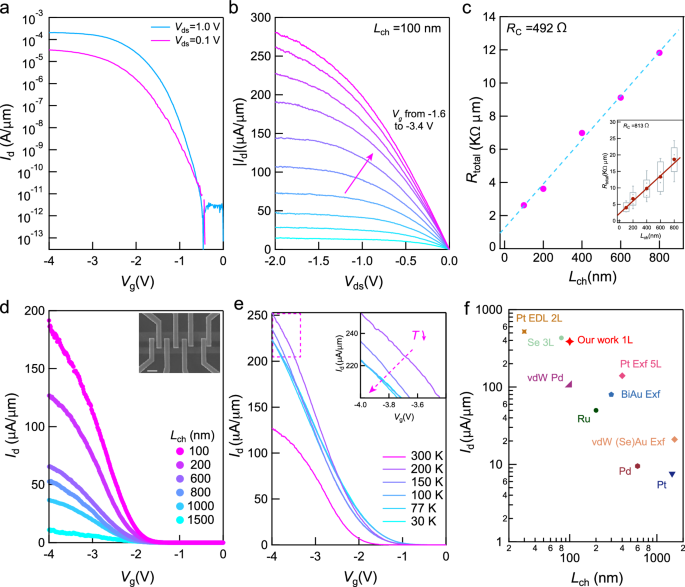
a Transfer curve of typical Au1-xSex – monolayer WSe2 contact with Lch = 100 nm under Vds = 1.0 V (blue line) and Vds = 0.1 V (pink line). Lch is the channel length, Vg is the gate voltage, Vds is the drain-to-source voltage, and Id is the drain current. b The output performance of the same device in a, for different gate voltage Vg ranging from −1.6 V to −3.4 V with −0.2 V step intervals. c Total resistance (Rtotal) as a function of Lch. The transfer-length-method (TLM) method is used for contact resistance (Rc) extraction. Inset: Boxplots of total resistance as a function of Lch for 6 TLM sets. The boxplot statistics were performed, showing mean (spot symbols), standard deviation, lower quartile (25%), median (50%), upper quartile (75%), interquartile range (25–75%). d Transfer curves of a typical TLM structure with Lch ranging from 0.1 μm to 1.5 μm and Vds = 1.0 V. Inset: scanning electron microscope image of a TLM structure. Scale bar, 2 μm. e Id–Vg of Au1-xSex –WSe2 at various temperatures from 300 K to 30 K. Inset: Zoom-in view of the transfer curves at Vg ranging from −4.0 V to −3.4 V. f Benchmark of Id vs. Lch of state-of-the-art contact approaches of WSe2 p-FETs without doping, Id at Vds = 1.0 V16,26,39,41,44,45,46,47,48.
To highlight the superior contact properties of Au1-xSex alloy, we conducted a performance comparison with direct Au metal contact configurations. As shown in the transfer characteristics in Supplementary Fig. 25, the typical Au1-xSex alloy layer as a band-aligned contact exhibits optimal electrical performance. As discussed earlier, the Se film forms a wetting layer at low-temperature and protects the surface of 2D TMDs. For direct Au contact with WSe2, high-energy Au atoms during deposition cause significant damage, inducing DIGS as shown in Fig. 1f, which limits the on-current to the microampere level, consistent with literature reports40. Clearly, the Au1-xSex alloy aligns closely with the VBM of WSe2, facilitating efficient hole injection for the p-branch. We also compared the device performance made from a contact film by depositing Au on a thicker Se buffer layer that has caused non-uniform Se residual as shown in Supplementary Fig. 25. Though the device performance is inferior compared to Au1-xSex alloy contact, it still demonstrates better performance than direct Au contacts.
The transfer-length-method (TLM) analysis43 from a particular device set is shown in Fig. 3c, which reveals a contact resistance (Rc) of ~492 Ω·µm for the Au1-xSex-WSe2 contact, consistent with the formation of clean vdW interface and the absence of Fermi-level pinning. Data from six sets of the TLM devices are shown in the inset with an average Rc of ~813 Ω·µm. Figure 3d compares the transfer performances across channel lengths (Lch = 100-1500 nm) measured via TLM devices, with an inset showing the corresponding SEM image (channel width = 1.0 μm).
When the temperature is lowered from room temperature (300 K) to 200 K, the drain current increases significantly as shown in Fig. 3e. From 200 K to 77 K, we observe a slight current attenuation. This phenomenon can be attributed to the competition between phonon scattering and thermionic emission mechanisms. In the range of 300 K to 200 K, thermionic emission of holes is sufficient to overcome the SB height, and phonon scattering dominates the transport behavior. The reduction in temperature significantly suppresses lattice scattering, leading to an increased hole mean free path and consequently enhanced current. However, when the temperature further decreases to below 200 K, the weakening of thermionic emission becomes the dominant limiting factor due to the presence of a small Schottky barrier, resulting in the observed current attenuation. Even when cooled to 30 K, the Au1-xSex-WSe2 contact device maintains a linear output curve (see Supplementary Fig. 26). This observation indicates that the ohmic contact is not yet perfect and a small SB height remains.
In Fig. 3f, we have benchmarked the Id vs. Lch performance of our devices against the best-reported p-type 2D TMD transistors employing various contact strategies. Our devices display a high current at 100 nm channel length16,26,39,41,44,45,46,47,48 than the previous record in p-type WSe2 solely through the evaporation method. Notably, while the best-performing devices in prior reports were typically based on multilayer (2 or 3 L) channels, our devices employ monolayer WSe2, which is more challenging to optimize, yet still achieve performance comparable to state-of-the-art multilayer devices. Furthermore, when compared with state-of-the-art p-FETs utilizing doping techniques, our devices still demonstrate strong competitiveness (refer to Supplementary Fig. 27)13,25,27,28,29,41,49,50.
Lastly, to validate the excellent uniformity and scalability of Au1-xSex-WSe2 contact p-FETs for large-scale integration, we fabricated 75 devices with varying channel lengths Lch and characterized their transfer characteristics, as shown in Fig. 4a. Statistical analysis of key device metrics reveals significant performance enhancement through channel length scaling. The statistical distributions of Ion, Vth, and SS as functions of channel length are systematically as quantified in Fig. 4b–d. The on-current Id increases from an average of 30 µA/µm to 200 µA/µm at Vg = −4.0 V with reducing Lch from 1000 nm to 100 nm. While some device-to-device variation is observed (attributed to batch-to-batch differences and WSe2 film quality variations), the consistent Ion improvement with scaling confirms the devices remain non-contact-limited, further evidencing the low contact resistance. Notably, the threshold voltage remains stable across scaled channels, while the subthreshold swing shows only minor degradation at Lch = 100 nm. This is a signature of short-channel effects likely originating from non-optimized 2D semiconductor/high-κ dielectric (HfO2) interfaces.
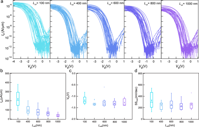
a Transfer characteristics of Au1-xSex–WSe2 p-FETs with channel lengths of 100 nm, 400 nm, 600 nm, 800 nm and 1000 nm under Vds = 1.0 V. b–d Boxplots of key device metrics, including on-current (Ion), threshold voltage (Vth), and subthreshold swing (SS). The color of the symbols corresponds to the channel length in a. For each group of data, the boxplot statistics were performed, showing mean (cross symbols), standard deviation, lower quartile (25%), median (50%), upper quartile (75%), interquartile range (25-75%).
In summary, we developed a Au1-xSex alloy contact strategy that overcomes Fermi-level pinning and defect-related challenges in p-type monolayer WSe2 transistors. The high work function (5.8 eV) and low-energy deposition process preserve the WSe2 lattice integrity. Through DFT calculations and STS measurements, we verified the suppression of interfacial gap states and a van der Waals gap of 2.5 Å, enabling quasi-ohmic contact with a low Schottky barrier. Devices exhibited low Rc (492 Ω·µm), high on-current (385 µA/µm), and high switching ratios (>108), outperforming conventional metal contacts. Statistical analyses confirmed excellent uniformity across scaled channel lengths (100–1000 nm), highlighting the approach’s viability for large-scale integration. This study provides a generalizable framework for contact engineering in 2D semiconductors, advancing the development of energy-efficient, post-silicon electronics.